SMT PCB Assembly: How It Works andWhy It Powers the Modern ElectronicsIndustry
Look around you. Your smartphone, your laptop, your smart TV, the fitness tracker on your wrist — every one of these devices contains a printed circuit board (PCB) packed with tiny electronic components. And the process that puts those components onto the board with such incredible precision and speed? That’s SMT PCB assembly. It’s one of the most important and widely used manufacturing processes in the electronics industry today, and understanding it can give you a real appreciation for the technology behind the devices we use every day.
In this article, we’ll walk you through everything you need to know about SMT PCB assembly — what it is, how it works, why it’s become the industry standard, and what trends are shaping its future.
What Is SMT PCB Assembly?
SMT stands for Surface Mount Technology. SMT PCB assembly is the process of attaching electronic components — known as Surface Mount Devices (SMDs) — directly onto the surface of a printed circuit board, where they are soldered in place to create electrical connections.
This is in contrast to the older through-hole technology (THT), where components had long wire leads that were inserted through holes drilled in the board and soldered on the underside. Through-hole assembly worked well for decades, but it was slow, space-inefficient, and not well-suited to the miniaturized, high-density designs that modern electronics demand.
SMT changed the game entirely. Surface mount components are much smaller, can be placed on both sides of the board, and are assembled using highly automated equipment that operates at remarkable speed and precision. This makes SMT PCB assembly the method of choice for producing everything from consumer gadgets to industrial equipment, medical devices, and telecommunications infrastructure.
The Key Components Used in SMT PCB Assembly
Before diving into the process itself, it helps to understand the types of components involved in SMT PCB assembly:
Resistors and Capacitors: These passive components are among the most common on any PCB. In SMT form, they are tiny rectangular chips available in standardized sizes such as 0402, 0603, and 0805 (measurements in hundredths of an inch).
Integrated Circuits (ICs): These are the “brains” of the circuit — microprocessors, memory chips, communication modules, and more. SMT ICs come in various packages such as QFP (Quad Flat Package), SOIC (Small Outline Integrated Circuit), and BGA (Ball Grid Array).
Transistors and Diodes: Used for switching, amplification, and signal control, these components are also available in compact SMT packages.
Connectors and Inductors: While some connectors still use through-hole mounting for mechanical strength, many are now available in SMT form as well.
The miniaturization of all these component types has been a key enabler of the compact, powerful devices we rely on today.
How Does SMT PCB Assembly Work?
SMT PCB assembly follows a well-defined sequence of steps, most of which are highly automated. Here’s a step-by-step look at the process:
Step 1: PCB Design and Preparation Everything starts with a well-designed PCB. Engineers create the board layout using CAD software, defining the size, shape, copper traces, and solder pads for each component. The design is then converted into manufacturing files — Gerbers for board fabrication, a Bill of Materials (BOM) for component procurement, and pick-and-place files that tell the assembly machines where each component goes.
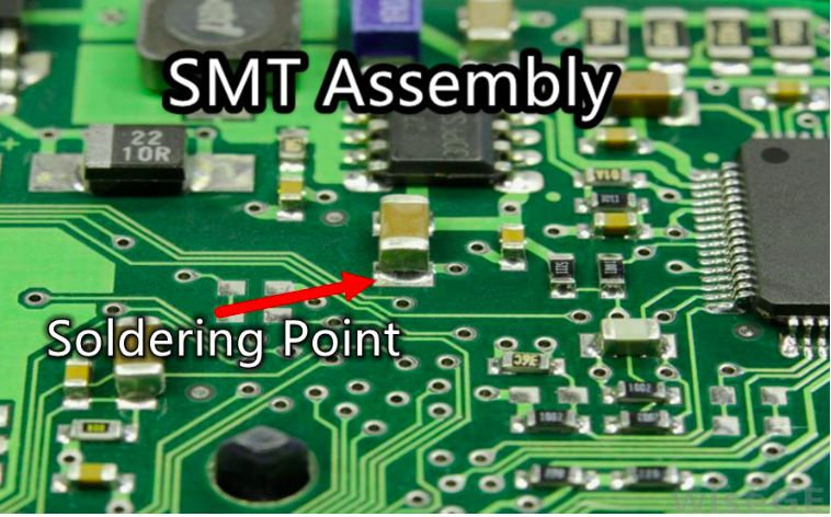
Step 2: Solder Paste Printing The first step on the production floor is applying solder paste to the bare PCB. A metal stencil — with openings that match the solder pads on the board — is placed over the PCB. A squeegee pushes solder paste through the openings, depositing a precise amount onto each pad. The quality of this step has a major impact on the final result; inconsistent paste application is one of the leading causes of soldering defects.
Step 3: Automated Component Placement With solder paste applied, the board moves to a pick-and-place machine — the workhorse of SMT PCB assembly. These automated systems use robotic arms equipped with vacuum nozzles to pick components from feeders (reels, trays, or tubes) and place them onto the solder paste with extraordinary precision. Modern pick-and-place machines can place tens of thousands of components per hour, using vision systems to verify correct placement before releasing each part.
Step 4: Reflow Soldering Once all components are placed, the board enters a reflow oven. The oven takes the board through a carefully controlled temperature profile with multiple zones — preheat, soak, reflow, and cooling. In the reflow zone, the solder paste reaches its melting point and flows around the component leads or pads, forming permanent, reliable solder joints. As the board cools, the solder solidifies and the connections are complete.
Step 5: Inspection After soldering, every board undergoes inspection to catch any defects. The most common method is Automated Optical Inspection (AOI), where high-resolution cameras scan the board and compare it against a reference image to detect issues like missing components, misalignment, solder bridges, or insufficient solder. For boards with BGA components — where solder joints are hidden beneath the package — X-ray inspection is used to see through the component and verify joint quality.
Step 6: Functional Testing Visual inspection alone isn’t enough. Functional testing verifies that the assembled board actually performs as intended. In-Circuit Testing (ICT) checks individual components and connections using a bed-of-nails fixture, while functional testing powers up the board and simulates real-world operating conditions to confirm overall performance.
Step 7: Rework and Touch-Up Boards that don’t pass inspection or testing are sent for rework. Skilled technicians use hot air rework stations, soldering irons, and microscopes to repair defects — replacing misplaced components, reflowing cold solder joints, or removing solder bridges — without damaging surrounding components.
Why SMT PCB Assembly Is the Industry Standard
The widespread adoption of SMT PCB assembly isn’t a coincidence. It offers a range of advantages that make it the clear choice for most modern electronics manufacturing:
Miniaturization: SMD components are dramatically smaller than through-hole equivalents, enabling the slim, compact designs consumers expect from modern devices.
Higher Component Density: Components can be placed on both sides of the board, and packed more closely together, allowing more functionality in less space.
Automation and Speed: The highly automated nature of SMT assembly means boards can be produced quickly and consistently, making it ideal for both high-volume production and fast-turnaround prototype runs.
Cost Efficiency: While setup costs for SMT equipment are significant, the speed and automation of the process result in lower per-unit costs at scale — a major advantage for mass production.
Improved Electrical Performance: Shorter electrical paths between components reduce inductance and resistance, improving signal integrity and high-frequency performance — critical for today’s fast processors and wireless communication chips.
Consistency and Reliability: Automated assembly reduces the variability introduced by manual processes, resulting in more consistent solder joints and higher overall reliability.
Common Challenges in SMT PCB Assembly
Despite its many advantages, SMT PCB assembly is not without its challenges:
Tombstoning: This defect occurs when one end of a small component lifts off the board during reflow, leaving it standing upright like a tombstone. It’s caused by uneven heating or imbalanced solder paste deposits and can be prevented through careful stencil design and process control.
Solder Bridging: When solder flows between two adjacent pads and creates an unintended connection, it’s called a solder bridge. This is particularly common with fine-pitch components and can cause short circuits.
Component Misalignment: Even with automated placement, components can shift slightly during reflow due to surface tension effects. Good stencil design, correct solder paste volume, and well-calibrated machines minimize this risk.
Thermal Management: Some components are sensitive to heat, and the high temperatures of lead free reflow soldering can stress or damage them if the temperature profile isn’t carefully controlled.
BGA Rework: Reworking BGA components — which have solder balls hidden beneath the package — is technically challenging and requires specialized equipment and skills.
SMT PCB Assembly Across Industries
SMT PCB assembly is used across virtually every sector of the modern economy:
Consumer Electronics: Smartphones, tablets, laptops, gaming consoles, and wearables all depend on SMT assembly for their compact, feature-packed circuit boards.
Automotive: Modern vehicles contain dozens of electronic control units (ECUs) for engine management, safety systems, infotainment, and driver assistance. SMT assembly produces these boards reliably and at the high volumes the automotive industry demands.
Medical Devices: From portable diagnostic equipment to implantable devices, medical electronics require the precision and miniaturization that only SMT can deliver.
Telecommunications: Base stations, routers, switches, and 5G infrastructure equipment all use high-performance PCBs assembled via SMT processes.
Industrial and Aerospace: Industrial automation controllers, robotics, and aerospace electronics rely on SMT PCBs for their durability, reliability, and performance in demanding environments.
Conclusion
SMT PCB assembly is the foundation of modern electronics manufacturing. Its combination of precision, speed, miniaturization, and cost efficiency has made it indispensable across virtually every industry that relies on electronic technology. As devices continue to evolve — getting smaller, faster, and more connected — SMT assembly will remain at the heart of how the world’s circuit boards are built. For companies looking to manufacture high-quality PCBs efficiently and at scale, partnering with an experienced provider of SMT PCB assembly in China offers access to world-class automated manufacturing facilities, deep process expertise, rigorous quality control, and the production capacity to meet the demands of even the most ambitious electronics projects.